Artis Fils, Hanna Maxie Brüggemann, Andrei Alexandru Popa (2025). From Composite Filaments to Low-loss Circuits: A Novel Hybrid Manufacturing Approach to 3D-Printed Electronics. In: Human Aspects of Advanced Manufacturing, Production Management and Process Control. AHFE Open Access, vol. 184, pp. 112–122. https://doi.org/10.54941/ahfe1006455
SDU Mechatronics, Centre for Industrial Mechanics, Institute of Mechanical and Electrical Engineering, University of Southern Denmark, 6400 Sønderborg, Denmark ↗
Electrically conductive filaments have shifted the paradigm of 2D circuitry towards 3D-printed electronics by enabling rapid prototyping of complex, embedded circuits. Despite being limited to low-current applications due to ohmic losses from their composite structure, the involvement of a user is kept at a minimum. Selective immersion-based electroplating addresses this limitation but is constrained to specific design spaces and requires human intervention. This study explores the concept and novelty of a proposed hybrid manufacturing system based on 3D printing followed by electroplating, addressing the limitations of traditional immersion-based methods. Moreover, both processes are performed on the same machine - a modified Prusa i3 MK3S+, paving the way towards sequential and human-independent hybrid manufacturing. Thusly 3D printed and electroplated samples were validated in terms of coating quality and their subsequent electrical resistance. The conductivity of commercially available copper-infused polymer filament was locally increased by two orders of magnitude through the proposed approach. Additionally, microscopy was used to characterize homogeneity. As a functional demonstrator, an electromagnetic acoustic transducer of 7.3 Ω resistance was successfully manufactured and tested, highlighting the practical applicability of the proposed method. Selective cup-based electroplating of 3D-printed electronics therefore announces its potential as a human-independent process within low-loss circuitry, while employing the full design-space flexibility of additive manufacturing.
The manufacturing of complex structures with greater design flexibility and shorter lead times has been made possible by polymer additive manufacturing (AM), which has had a transformative impact on various industries (Godec et al., 2024). Over the past few decades, AM has garnered significant attention in several sectors, including aerospace, automotive, medical, and electronics (Ngo et al., 2018). Fused Filament Fabrication (FFF), a method of AM, is a popular form of thermoplastic extrusion, which stands out as cost- efficient means of rapid prototyping (Ferretti et al., 2022). Thermoplastic composites containing a variety of doping materials, including metals, ceramics, carbon nanotubes, and biomaterials, have been developed in
response to the growing demand for functional materials (Park & Fu, 2021). Electrically conductive thermoplastic composites present great opportunities and applications in wearable electronics, human motion sensors, health monitoring, or soft robotics fields (Criado-Gonzalez et al., 2021).
The content of electrically conductive additive greatly impacts the resulting composites resistivity (Guo et al., 2019). The state-of-the-art commercially available conductive filament “Electrifi” claims resistivity of 6.0 · 10−3 [ · cm] (Multi3D, 2024). For reference, copper, as the traditional material of choice for electrically conducting applications, exhibits lower resistivity (1.68 · 10−6 [ · cm]) (Duhain et al., 2021). This renders it suitable for low-ohmic-loss applications, such as motor control, electromagnetic devices such as antennas. Hence, there exists ample research in metal coating methods for non-metallic surfaces (Akhouri, Banerjee and Mishra, 2020; Equbal and Sood, 2014; Fotovvati, Namdari and Dehghanghadikolaei, 2019; Tushinsky et al., 2002; Alghamdi et al., 2021). Coatings can be selectively applied, targeting specific areas of a component, albeit restricted to outer surfaces, as is the case with, for instance, brush plating. As an alternative to the direct manufacturing of electrically conductive substrates, electroplating consists of depositing a layer of conductive metal that fuses to a conductive substrate. This method of coating that often includes an FFF 3D printer, has witnessed increased popularity in recent years, with several research groups undertaking efforts in both electroplating (Angel et al., 2018; Augustyn et al., 2021; Filonov et al., 2019; Gerges et al., 2023; Lazarus et al., 2019) and electroless plating (Dixit, Srivastava and Narain, 2017; Ishikawa et al., 2017; Lazarus et al., 2022; Li et al., 2019; Zhan et al., 2020). The process of electroplating, with its low-cost and relative ease of implementation, especially for metals such as copper (Le et al., 2015), makes the object of this study.
A common improvement point for all previous research efforts is linked to submerged plating approach, which hinders the potential of sequential 3D printing and electroplating steps. Specifically, printing a submerged environment imposes several process and device challenges (Korniejenko et al., 2024). To address these shortcomings, the current effort seeks to lay the groundwork for a non-submerged sequence of 3D printing and electroplating, along with the option of selectively alternating between the two processes. A 2-step process was commonly observed in literature. The first step typically consists of 3D printing a layer of polymer or polymers, followed by the coating as the second step. This sequence is performed with operator intervention, which leads to increased cost and risk of human error. The 2-step process, with its submerged coating, generally studied in literature further limits the design space of AM electro-mechanical components, due to a loss of possible encapsulation. Therefore, this study will focus on enabling low-cost, semi-autonomous, low-ohmic-loss applications via electroplating for FFF manufacturing. In consequence, materials are usually sourced from commercially available providers.
MATERIALS AND METHODS
This study focusses on the static anode electroplating, which induces different distances and a wide gradient of resistances between the anode and the to-be- coated surface. This issue is addressed in the study from Kim, et al. on one- step electrodeposition of copper on different conductive filaments (Kim et al., 2019), where the solution is to use a lower resistivity filament. Multi3D’s Electrifi High Temp Conductive Filament was chosen as the conductive filament, due to having the most uniform copper electrodeposits, which leads to the lowest resistivity. Alternatives such as in-house manufactured filament were not considered due to the extensive supporting research and commercial availability of Electrifi. As for the substrate filament, which would be bonding to the Electrifi, 3DE Premium PETG was chosen, as this thermoplastic is suggested by the manufacturer.
Since the scope of this study was not to develop an electrolyte solution or any proprietary materials, but rather focus on the hybrid manufacturing process, a commercially available solution for the former was chosen under the form of Dr. Galva’s Bright Copper coating solution. For the electroplating process, copper tubing was used as an anode, with its hole serving the purpose of depositing and retracting electrolyte. The anode is attached to a syringe, which acts as an electrolyte reservoir allowing both controlled deposition and retraction of the solution. As for the cathode, a copper foil tape was added to a textured build plate of a FFF machine. To ensure proper current flow a GW Instek GPS-3303 power supply was used. As the being-printed part is being held in place by the adhesion to the conductive build plate, the anode with the syringe was held by a generic adjustable lab stand with a clamp.
Manufactured parts were designed in Siemens NX, in two different solid bodies, one as the conductive and the other as the non-conductive. This enables multi-material slicing without the use of a dual material handling system and multi-material painting. CAD model was imported into PrusaSlicer, where with the use of virtual extruders, multi material g-code was possible, with only one physical extruder. For the FFF process, a Prusa MK3S+ was used.
Resistance was measured with Fluke 179 True-RMS digital multimeter. SEM analysis was performed with Keyence VHX-5000 digital microscope. Validation of the hybrid manufacturing was done by a use case – electromagnetic acoustic transducer (EMAT). An electromagnet was manufactured by the proposed manufacturing process, while a Ø60 mm by 5 mm permanent magnet was purchased from Supermagnete. Raspberry Pi 4 and an Adafruit I2S 3W Stereo Speaker Bonnet were used to generate a sound signal for the EMAT. The acoustics were recorded by a OnePlus Nord CE with the built-in Recorder app, finally a python script was used to generate a spectrogram.
RESULTS & DISCUSSION To avoid the drawbacks of submerged electroplating, an alternative methodology is proposed. An electrolyte can be deposited in a controlled amount and area, to perform the electroplating, after which the solution
From Composite Filaments to Low-Loss Circuits 115
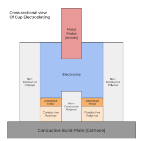
is retracted. In result, the machine reaches a state where printing could be resumed, due to the removal of the electrolyte and anode. To achieve this, it is necessary to consider an appropriate method for containing the electrolyte in the desired area. Ideally, the electrolyte can be contained due to the inherent surface tension, which wouldn’t add any specific conditions before electroplating commences. To validate the setup, specifically with the copper- foil-covered build plate acting as a cathode, the adherence and consequential electrical connection between the former and the conductive thermoplastic was qualified. Disregarding the amount of electrolyte needed, initial efforts employed non-conductive polymer walls, to create a cup-based structure for containing the electrolyte. Figure 1 depicts a cross-sectional view illustrating the key points of the cup-based approach.
Figure 1: Simplified illustration of cup-based electroplating.
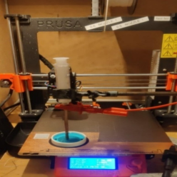
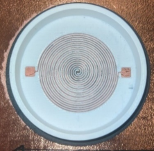
The middle column of non-conductive polymer is higher than the conductive polymer, which ensures that the coating can only be deposited as a vertical build-up on top of the conductive polymer. If it were not the case, it could potentially lead to the coating spreading laterally which could interfere with the polymer deposition after coating. After performing the process shown in Figure 2, a specimen was successfully manufactured, as shown in Figure 3.
Figure 2: Active electroplating process after the 3D printing step.Figure 3: Successfully manufactured spiral specimen.
Characterization and Validation of the Process To validate and characterize the approach, nine specimens were manufactured, with controlled variations in coating time and current density, and one uncoated specimen was manufactured as a reference. The coating parameters are a combination of these three current densities: 0.05 mA/mm2, 0.15 mA/mm2 and 0.25 mA/mm2 in combination with a coating time of 30 minutes, 1 hour and 2 hours.
To prove copper is deposited on the surface, its amount is characterized by weighing the specimen before and after electroplating. While the geometry, specifically the thickness, and the density of the coated layer are not characterized, the increase in mass is indicative of the success of the method. The homogeneity is evaluated using microscopy images of the specimens in different locations. This allows a comparison between the different coating parameters and the coating outcome connected to it as well as a visualisation of the coating gradient that is spreading from the anode in the center of the specimen. This coating gradient is also quantified in the resistance throughout the traces. Reducing this gradient is desirable to have a homogeneous conductivity through the full specimen enabling safe and reliable application e.g. avoiding localized current concentrations, which could lead to excessive Joule heating.
The coating process of the specimen coated at a current density of 0.25 mA/mm2 were not completed ideally since the deposited copper bonded the anode to the coating surface which short-circuited the coating process. It is unclear if any coating still took place after this point so the results from this specimen are not representable.
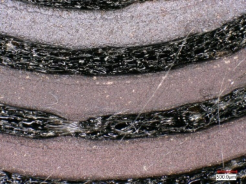
Figure 4: Microscopy image of the specimen (1 h-0.25 mA/mm2) in the center position.
From Composite Filaments to Low-Loss Circuits 117
Figure 5: Microscopy image of specimen (1h-0.15 mA/mm2) of three traces.
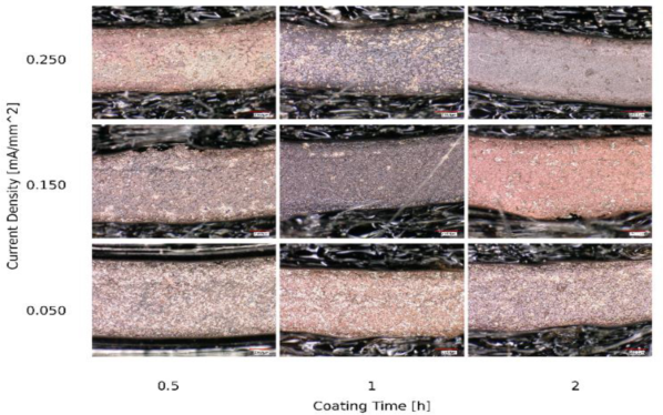
Microscopy pictures of the specimens were taken at different locations to evaluate the coating quality as well as to visualize the coating gradient. All specimens display a gradient in the coating quality from the center to the outside of the specimen as shown in Figure 5 of one specimen as well as in Figure 4 showing the higher deposition in the center. The overall coating homogeneity improves with an increase in coating time and current density as shown in the overview in Figure 6. This is most visible when comparing the specimen coated for two hours. The coating with a current density of 0.15 mA/mm2 is more homogeneous than the specimen coated at a lower current density. The specimens coated under a current density of 0.25 mA/mm2 are less depictive due to the imperfect coating.
Figure 6: Microscopy image of all specimens in the Trace position with 0.25mm scale.
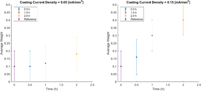
When comparing the specimen weight over different coating times, it is visible through all coating densities, that the amount of copper deposited increases over time as plotted in Figure 7. An increase in current density also leads to an increase in deposited copper as evident when comparing the specimens coated with a current density of 0.05 mA/mm2 and 0.15 mA/mm2 for 2 hours. Figure 7 does not include data from the 0.25 mA/mm2 samples, due to the aforementioned imperfections.
Figure 7: Graph showing the weight of specimen based on different coating parameters.
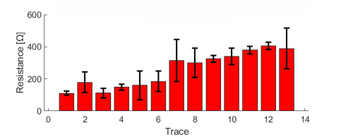
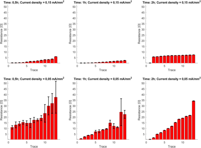
The resistance was measured from the center to each trace along the windings of the spiral to characterise the coating gradient as well as the impact of the coating parameters on the resistance, as visualised in Figure 9. An uncoated reference specimen is measured and illustrated by Figure 8, highlighting the improvement induced by the coating process. It can be noticed that the variation in resistance of the uncoated specimen is large due to the inhomogeneous nature of doped conductive filament and its low hardness. The filament is a copper infused polyethylene whose conductivity is greatly impacted by printing orientation.
Figure 8: Resistance based on trace for an uncoated specimen.
The specimens coated using a current density of 0.05 mA/mm2 reveal less fluctuation in measurements as coating time increases. This is due to the copper forming a more rigid surface and with that a more stable connection to the multimeter. It can be noticed that with a higher current density, the resistance decreases due to the coating becoming more homogenous.
From Composite Filaments to Low-Loss Circuits 119
Figure 9: Resistance based on the measured trace from the center.
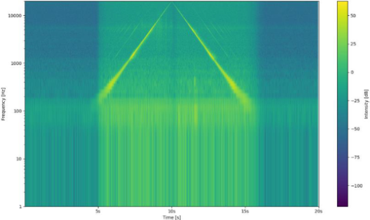
Functional Demonstrator–Electromagnetic Acoustic Transducer An electromagnetic acoustic transducer (EMAT) was chosen as the functional demonstrator, proving that the coating enables higher current applications. A round Archimedean spiral was chosen, to minimize the sharp corners, which could induce localized disruptions in current flow due to increased resistive effects. The specific spiral will lead to more uniform current concentration, positively impacting the uniformity of the electromagnetic field. Accompanying the round spiral, the permanent magnet is also of a similar diameter circular cross-section, yielding matching fields. The spacing between the traces, should be kept to a minimum, to increase the density of the traces for a more uniform electromagnetic field, restricted to 0.6 mm due nozzle size requirements for the Electrifi filament. As the selected DAC supports 3W at 5V, the maximum current the electromagnet must handle 0.6 A at a resistance between 4 and 8 . Prior experiments indicated that a single line width of a 0.6 mm nozzle created nonuniform coating, therefore the lined width was chosen as 1.2 mm. By measuring resistance from previous specimens, 18 turns were empirically linked to 7 resistance within the spiral geometry. After designing and manufacturing, the resulting specimen had the measured resistance of 7.3 . Wires were soldered on to the trace, to ensure a robust connection. With the permanent magnet at 5 mm from the electromagnet and the microphone at 5 mm from the electromagnet, a frequency sweep starting from 1 Hz to 20k Hz finally to 1 Hz over 20 seconds was played and recorded for analysis. The recorded audio file was converted to a spectrogram, found in Figure 10.
Figure 10: Logarithmic spectrogram of a frequency sweep.
It has been found that only frequencies above 140.6 Hz, were successfully recorded. Multiple resonance lines can be found in the interval from 500 Hz to 2k Hz. It must be acknowledged that the smartphones frequency curve does impact the frequency response curve, although it still proves the overarching goal of achieving an audible sound.
CONCLUSION & FURTHER IMPROVEMENTS This study has successfully demonstrated a novel hybrid manufacturing method to produce 3D printed circuitry for higher current applications. The proposed cup-based electroplating method simplifies the combination of FFF and electroplating. The weight measurements lead to the conclusion, that the copper is successfully deposited in the hybrid approach. Microscopy indicates a uniform yet uneven coating surface. The coating exhibits a gradient, as more copper gets deposited around the anode – which leaves room for future improvement. The resistance measurements led to the conclusion that low-ohmic-loss applications are possible. The functional demonstrator – electromagnetic acoustic transducer was successfully manufactured and tested. A spectrogram of the frequency sweep test illustrated the successfully transduced frequencies and their respective decibel levels, which validates the practical applicability of the proposed hybrid approach. Further development in the dynamic anode would address the issues associated with the gradient- like deposition of copper. Selective cup-based electroplating of 3D-printed electronics shows the promise in human-independent process that enables low-loss applications without compromising the design-space flexibility of additively manufacturing electronics.
ACKNOWLEDGMENT
The authors would like to acknowledge the Bitten Mads Clausens Fond for supporting the hardware used in this effort, along with Casper Kunstmann and Fatma Nur Depboylu for their input and help with testing and characterization.
From Composite Filaments to Low-Loss Circuits 121
REFERENCES
Akhouri, D., Banerjee, D. and Mishra, S. B. (2020) ‘A review report on the plating process of fused deposition modelling (FDM) built parts’, Materials Today: Proceedings, 26, pp. 2140–2142. https://doi.org/10.1016/J.~MATPR.2020.02. 461. Alghamdi, S. S. et al. (2021) ‘Additive Manufacturing of Polymer Materials: Progress,
Promise and Challenges’, Polymers 2021, Vol. 13, Page 753, 13(5), p. 753. https: //doi.org/10.3390/POLYM13050753. Angel, K. et al. (2018) ‘Selective electroplating of 3D printed parts’, Additive Manufacturing, 20, pp. 164–172. https://doi.org/10.1016/J.~ADDMA.2018.01. 006. Augustyn, P. et al. (2021) ‘A review on the direct electroplating of polymeric
materials’, Journal of Materials Science, 56(27), pp. 14881–14899. https://doi. org/10.1007/S10853-021-06246-W/FIGURES/3. Criado-Gonzalez, M. et al. (2021) ‘Additive Manufacturing of Conducting Polymers: Recent Advances, Challenges, and Opportunities’, ACS Applied Polymer Materials, 3(6), pp. 2865–2883. https://doi.org/10.1021/ACSAPM.1C00252/AS SET/IMAGES/LARGE/AP1C00252_0007.~JPEG. Dixit, N. K., Srivastava, R. and Narain, R. (2017) ‘Electroless Metallic Coating
on Plastic Parts Produced by Rapid Prototyping Technique’, Materials Today: Proceedings, 4(8), pp. 7643–7653. https://doi.org/10.1016/J.~MATPR.2017.07. 098. Duhain, A., Lamblin, G. and Lenoble, D. (2021) ‘On the resistivity, temperature coefficient of resistance, and ampacity of Cu–CNT and Ni–CNT composites’, RSC Advances, 11(63), pp. 40159–40172. https://doi.org/10.1039/D1RA07048G. Equbal, A. and Sood, A. kumar (2014) ‘Metallization on FDM Parts Using the
Chemical Deposition Technique’, Coatings 2014, Vol. 4, Pages 574–586, 4(3), pp. 574–586. https://doi.org/10.3390/COATINGS4030574. Ferretti, P. et al. (2022) ‘Production readiness assessment of low cost, multi-material, polymeric 3D printed moulds’, Heliyon, 8(10), p. e11136. https://doi.org/10. 1016/J.~HELIYON.2022.~E11136. Filonov, D. et al. (2019) ‘Volumetric 3D-Printed Antennas, Manufactured via
Selective Polymer Metallization’, physica status solidi (RRL) – Rapid Research Letters, 13(6). https://doi.org/10.1002/PSSR.201800668. Fotovvati, B., Namdari, N. and Dehghanghadikolaei, A. (2019) ‘On Coating Techniques for Surface Protection: A Review’, Journal of Manufacturing and Materials Processing 2019, Vol. 3, Page 28, 3(1), p. 28. https://doi.org/10.3390/ JMMP3010028. Gerges, T. et al. (2023) ‘Rapid 3D-Plastronics prototyping by selective metallization
of 3D printed parts’, Additive Manufacturing, 73, p. 103673. https://doi.org/10. 1016/J.~ADDMA.2023.103673. Godec, D. et al. (2024) ‘Introduction to Additive Manufacturing’, Springer Tracts in Additive Manufacturing, Part F3252, pp. 1–44. https://doi.org/10.1007/978-3- 031-05863-9_1/FIGURES/23. Guo, R. et al. (2019) ‘Electrical and Thermal Conductivity of Polylactic Acid (PLA)-
Based Biocomposites by Incorporation of Nano-Graphite Fabricated with Fused Deposition Modeling’, Polymers 2019, Vol. 11, Page 549, 11(3), p. 549. https: //doi.org/10.3390/POLYM11030549. Ishikawa, A. et al. (2017) ‘Selective electroless plating of 3D-printed plastic structures for three-dimensional microwave metamaterials’, Applied Physics Letters, 111(18). https://doi.org/10.1063/1.4986203/34233.
Kim, M. J. et al. (2019) ‘One-step electrodeposition of copper on conductive 3D printed objects’, Additive Manufacturing, 27, pp. 318–326. https://doi.org/10. 1016/j.addma.2019.03.016. Korniejenko, K. et al. (2024) ‘Additive Manufacturing in Underwater Applications’,
Applied Sciences 2024, Vol. 14, Page 1346, 14(4), p. 1346. https://doi.org/10. 3390/APP14041346. L. I. Tushinsky et al. (2002) Coated Metal: Structure and Properties of Metal-Coating Compositions. Springer. Lazarus, N. et al. (2019) ‘Selective Electroplating for 3D-Printed Electronics’,
Advanced Materials Technologies, 4(8), p. 1900126. https://doi.org/10.1002/AD MT.201900126. Lazarus, N. et al. (2022) ‘Direct electroless plating of conductive thermoplastics for selective metallization of 3D printed parts’, Additive Manufacturing, 55, p. 102793. https://doi.org/10.1016/J.~ADDMA.2022.102793. Le, N. N. et al. (2015) ‘Optimization of copper electroplating process applied for
Multi3D. All Rights Reserved. https://www.multi3dllc.com/product/electrifi-high- temp/ (Accessed: 3 June 2024). Ngo, T. D. et al. (2018) ‘Additive manufacturing (3D printing): A review of materials, methods, applications and challenges’, Composites Part B: Engineering, 143, pp. 172–196. https://doi.org/10.1016/J.~COMPOSITESB.2018.02.012. Park, S. and Fu, K. (Kelvin) (2021) ‘Polymer-based filament feedstock for additive
manufacturing’, Composites Science and Technology, 213, p. 108876. https://do i.org/10.1016/J.~COMPSCITECH.2021.108876. Zhan, J. et al. (2020) ‘Metal-plastic hybrid 3D printing using catalyst-loaded filament and electroless plating’, Additive Manufacturing, 36, p. 101556. https://doi.org/ 10.1016/J.~ADDMA.2020.101556.
LISTED IN THE AHFE DIGITAL BOOKSTORE CATALOGUE
Explore the complete digital volume
Human Aspects of Advanced Manufacturing, Production Management and Process Control
Read this individual research paper free through the original publisher, or explore the full digital proceedings book.
ISBN 978-1-964867-60-1
Explore this ISBN in the AHFE Bookstore ↗Listed in the July 2026 bookstore catalogue; search by ISBN to confirm current availability · Digital book purchase optional